Η All-in-One Λύση για τα Δεδομένα της Επιχείρησής σας
Όλα τα KPIs σας σε ένα σημείο. Δείτε καθαρά την πορεία της επιχείρησής σας, βελτιώστε την απόδοσή σας και επικεντρωθείτε σε αυτό που μετράει: την ανάπτυξη.
★★★★★
Το εμπιστεύονται πάνω από 50 Επιχειρήσεις & Agencies


ΟΛΑ ΟΣΑ ΧΡΕΙΑΖΕΣΤΕ
Τα Κλειδιά της Επιτυχίας
Reporting
Παρακολουθήστε τις επιδόσεις σας σε πραγματικό χρόνο.
Forecast
Αναλύστε τάσεις και κάντε προβλέψεις για στρατηγικές αποφάσεις.
Benchmarks
Συγκρίνετε την πρόοδό σας με την αγορά.
Integrations
Διασύνδεση με πάνω από 100 πλατφόρμες για να φέρετε όλα τα δεδομένα τις επιχείρησης σας σε ένα μέρος.


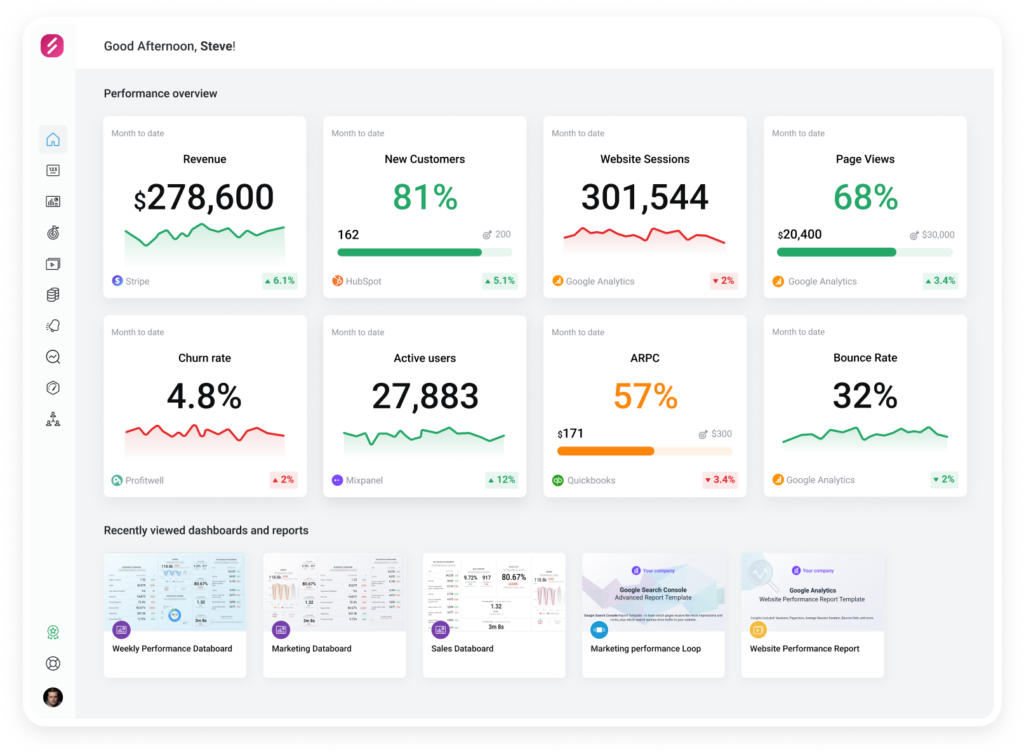
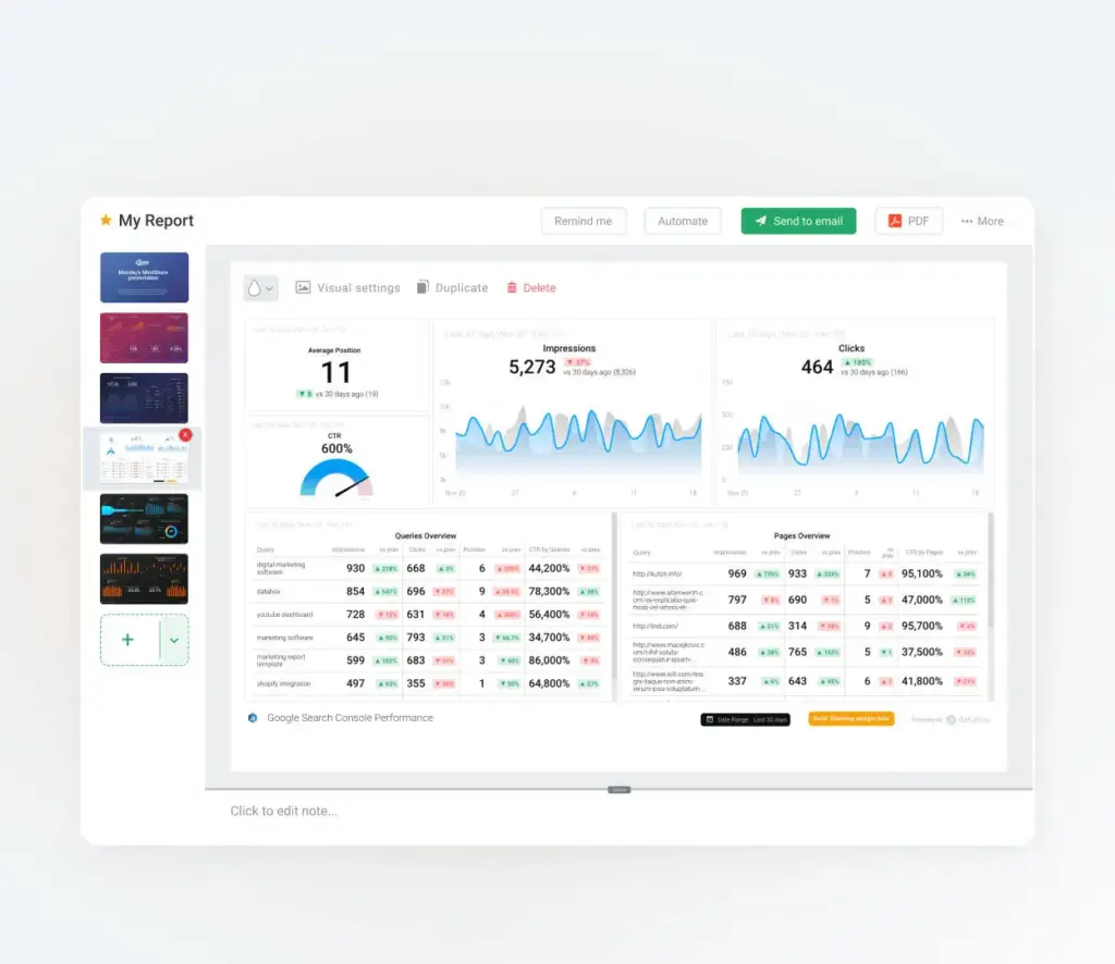
Reporting που δίνει νόημα στα δεδομένα σας
Οι αναφορές σας είναι συγκεντρωμένες, εύκολα κατανοητές και προσαρμόσιμες στις ανάγκες σας. Παρακολουθήστε όλα τα KPIs και τις μετρήσεις από διαφορετικά κανάλια σε μία ολοκληρωμένη προβολή, ώστε να μπορείτε να δείτε την πραγματική εικόνα της επιχείρησής σας χωρίς να χάνετε χρόνο με αναλύσεις. Αυξήστε την παραγωγικότητα της ομάδας σας, λαμβάνοντας τις πληροφορίες που χρειάζεστε, όποτε τις χρειάζεστε.
- Custom Metrics
- Drag and Drop Builder
- Real Time Data
- Εξοικονόμηση Χρόνου
AI Overview
All the tools you need
Templates
Made for everyone
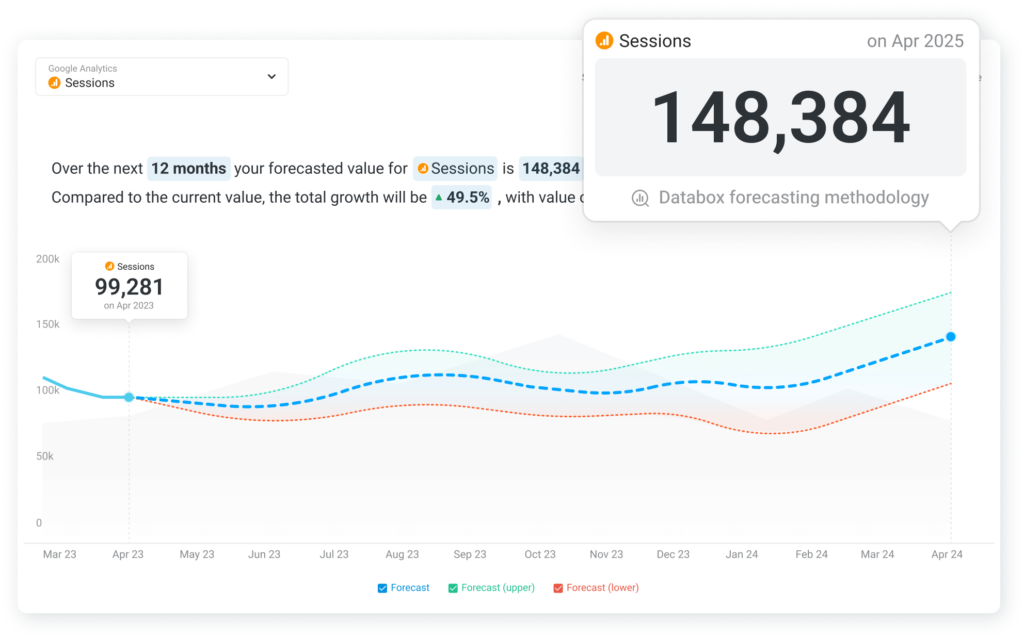
Forecast Report
Το benchmarks.gr σας επιτρέπει να προβλέψετε κρίσιμες τάσεις και να σχεδιάσετε στρατηγικά βήματα με βάση τα δεδομένα σας. Αναλύστε τα ιστορικά στοιχεία σας και προβλέψτε τη μελλοντική σας πορεία με μεγαλύτερη ακρίβεια. Με διαδραστικές προβολές και παραμετροποιημένα insights, μπορείτε να εντοπίσετε ευκαιρίες ανάπτυξης, να προσαρμόσετε τους στόχους σας και να προετοιμάσετε την ομάδα σας για το επόμενο βήμα.
- Προβλέψεις Βασισμένες σε Δεδομένα
- Διαδραστικά Γραφήματα
- Ανάλυση Τάσεων
- Ευθυγράμμιση Στόχων
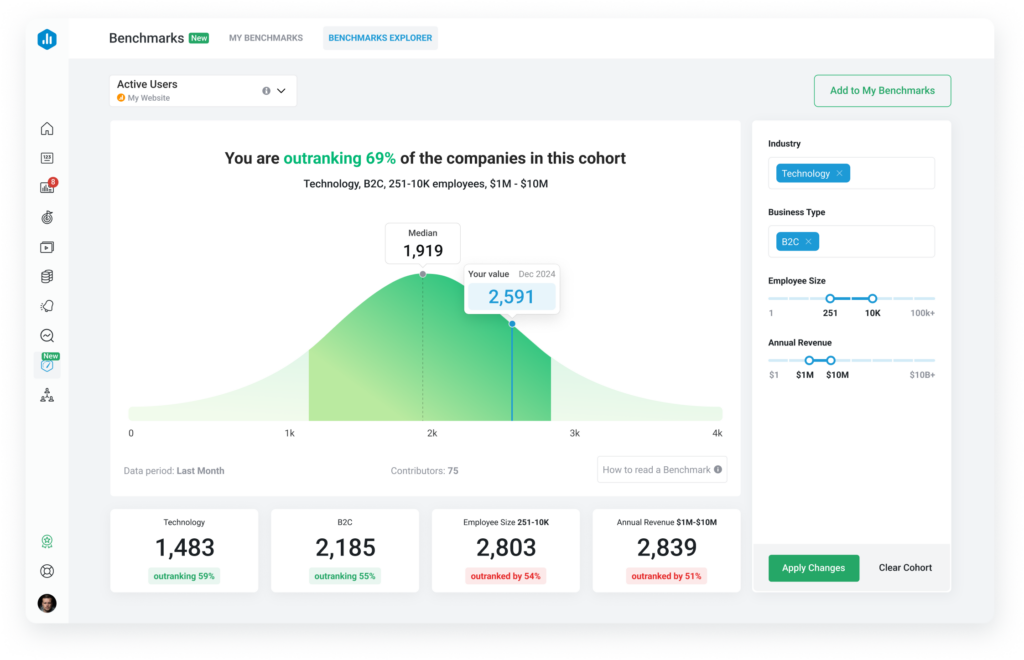
Συγκρίνετε την Απόδοσή σας με τα δεδομένα της Αγοράς
Αποκτήστε πρόσβαση σε αξιόπιστες συγκρίσεις και αναφορές που σας δείχνουν πώς συγκρίνεται η επιχείρησή σας με τον ανταγωνισμό και την αγορά. Κατανοήστε τα δυνατά σας σημεία, εντοπίστε περιοχές για βελτίωση και βάλτε στόχους που οδηγούν σε καλύτερη απόδοση. Μέσω των αναλυτικών benchmarks, μπορείτε να πάρετε αποφάσεις που ενισχύουν την ανάπτυξη, παρακολουθώντας την πρόοδο της επιχείρησής σας σε πραγματικό χρόνο.
- Συγκρίσεις με τον Ανταγωνισμό
- Ανάλυση σε Πραγματικό Χρόνο
- Εντοπισμός Ευκαιριών Βελτίωσης
- Θέστε Στόχους Ανάπτυξης
FAQs
Συχνές ερωτήσεις
Τι είναι το benchmarks.gr;
Ποιος είναι ο στόχος του Benchmarks;
Χρειάζομαι προηγούμενη εμπειρία με analytics για να χρησιμοποιήσω το benchmarks.gr;
Είναι το benchmarks.gr συμβατό με άλλες πλατφόρμες ή εργαλεία που χρησιμοποιώ ήδη;
Γιατί το Χρειάζεστε;
Ποιες επιχειρήσεις θα επωφεληθούν περισσότερο από το benchmarks.gr;
Πώς μπορώ να ξεκινήσω;
Read more
- Προηγμένα KPIs & Reporting στο E-commerce: AI, Προγνωστική Ανάλυση & Ολιστική Στρατηγική για το 2025+
- E-commerce Analytics & Reporting 2025: Πώς να Ενώσετε Δεδομένα & Στρατηγική για Απογείωση των Πωλήσεων
- Αποκρυπτογραφώντας το Conversion Rate: Εργαλεία & Τεχνικές που θα αλλάξουν τα eShop το 2025
- 10 Κορυφαίες Τάσεις στο Reporting για το 2025
- Benchmarking στην Επιχείρηση: Στρατηγικές για Καλύτερη Απόδοση
Είστε έτοιμοι να πάρετε τις καλύτερες αποφάσεις για την επιχείρησή σας;
Αξιοποιήστε τα δεδομένα για κάθε σας απόφαση.
- Προηγμένα KPIs & Reporting στο E-commerce: AI, Προγνωστική Ανάλυση & Ολιστική Στρατηγική για το 2025+
- E-commerce Analytics & Reporting 2025: Πώς να Ενώσετε Δεδομένα & Στρατηγική για Απογείωση των Πωλήσεων
- Αποκρυπτογραφώντας το Conversion Rate: Εργαλεία & Τεχνικές που θα αλλάξουν τα eShop το 2025
- 10 Κορυφαίες Τάσεις στο Reporting για το 2025
- Benchmarking στην Επιχείρηση: Στρατηγικές για Καλύτερη Απόδοση